Stacked tape carrier is a method for interconnecting ICs using TAB technology. This method could be divided further into stacked TAB on PCB and stacked TAB on leadframe as illustrated by the schematic diagram shown in Figure ![]() .
.
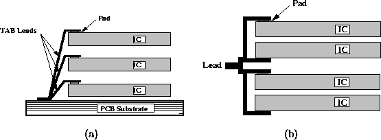
Figure: Two variants of the stacked tape carrier vertical interconnect. (a) Stacked TAB on PCB. (b) Stacked TAB on Leadframe.
The TAB on PCB method is used by Intel Japan and Matsushita Electric Industrial Company. In Matsushita's case, they used this approach for designing high density memory cards. The second method is used by Fujitsu in designing 4 Mbit DRAM chips.