Advances in interconnection technology have played a key role in allowing continued improvement in integrated circuit density, performance, and cost. Over the last 20 years circuit density has increased by a factor of approximately ![]() . According to Gordon Moore, CEO of Intel, integrated circuits will roughly double in density every device generation, resulting in a straight-line on a log scale as shown in Figure
. According to Gordon Moore, CEO of Intel, integrated circuits will roughly double in density every device generation, resulting in a straight-line on a log scale as shown in Figure ![]() [27]. It turns out that each technology generation lasts about 18 months. As a result, feature size and resolution of geometries used in production follow the same trend with feature size reductions of about 20% per component generation. At the same time, increased functional integration has lead to larger chip sizes - this has lead to increased wafer size and the requirement for equipment to handle larger wafers.
[27]. It turns out that each technology generation lasts about 18 months. As a result, feature size and resolution of geometries used in production follow the same trend with feature size reductions of about 20% per component generation. At the same time, increased functional integration has lead to larger chip sizes - this has lead to increased wafer size and the requirement for equipment to handle larger wafers.
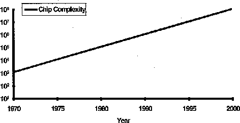
Figure: Moore's Law for active element density. The y - axis refers to the number of transistors per unit area (1 mm ![]() )
)
Currently, increasing numbers of integrated circuits are packaged in 2D and 3D forms, with increasing overall system complexity. A large number of systems have been implemented using the 2D form, and have demonstrated that such complexity can be managed. However, a fewer number of systems and devices have been implemented using 3D technology, proving nevertheless that such devices or systems are manageable, although complex. Managing complex systems, from a systems designer point of view, is achieved by designing and developing software to cope with the increasing system complexity.