Wire bonding is a method used to connect a fine wire between an on-chip pad and a substrate pad. This substrate may simply be the ceramic base of a package or another chip. The structure of a wire bond assembly is shown in Figure ![]() . Common wire materials include gold and aluminium.
. Common wire materials include gold and aluminium.
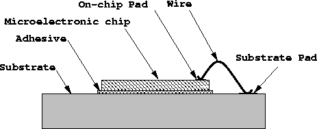
Figure: The wire bonding assembly shows how a bare chip is interconnected to a substrate or another chip using a wire conductor. Hence, the `substrate pad' may either be a package pad or a pad on another chip.
The main advantage of wire bonding technology is that it is low-cost. The disadvantages include (a) low I/O counts due to technology limitations, (b) large bonding pads in the order of 100 ![]() 100
100 ![]() m
m ![]() , (c) large bonding pitch
, (c) large bonding pitch![]() in the order of 200
in the order of 200 ![]() m, (d) the requirement for relatively large quantities of gold, (e) production rate, (f) relatively poor electrical performance, (g) variations in bond geometry and (h) robustness and reliability problems brought about by environmental conditions.
m, (d) the requirement for relatively large quantities of gold, (e) production rate, (f) relatively poor electrical performance, (g) variations in bond geometry and (h) robustness and reliability problems brought about by environmental conditions.