Tape-automated bonding (TAB) is an approach to fine the pitch interconnection of a chip to a leadframe. The interconnections are patterned on a multilayer polymer tape. The tape is positioned above the `bare die' so that the metal tracks (on the polymer tape) correspond to the bonding sites on the die, as shown in Figure ![]() . A new version of TAB, referred to as `area TAB', borrows a good idea from a bonding technique called `bump bonding' (which will be discussed in section
. A new version of TAB, referred to as `area TAB', borrows a good idea from a bonding technique called `bump bonding' (which will be discussed in section ![]() ). In this version, metal bumps are distributed over the entire surface of the chip (ie. I/O and power/ground terminals are not constrained to the chip periphery) - thus a large I/O count becomes viable.
). In this version, metal bumps are distributed over the entire surface of the chip (ie. I/O and power/ground terminals are not constrained to the chip periphery) - thus a large I/O count becomes viable.
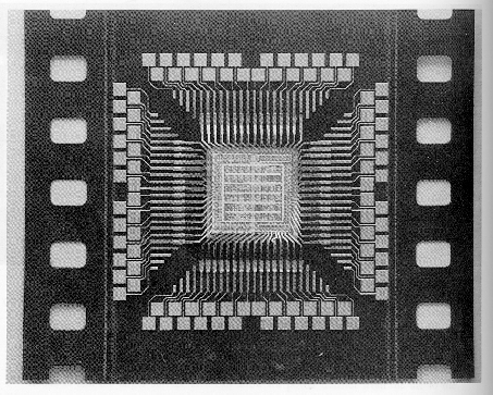
Figure: Tape-automated bonded die with a bare chip placed on the tape and connected to an interconnection pattern (Courtesy of Westinghouse ESG).
The tape-automated bonding technology provides several advantages over the wire bonding technology. These advantages include (a) a smaller bonding pad compared to wire bonding technology, (b) smaller on-chip bonding pitch in the range of 100 ![]() m, (c) a decrease in the quantity of gold used for bonding, (d) the reduction of variations in bond geometry, (e) an increase in production rate because of area or `gang' bonding, and (f) a stronger and more uniform inner lead bonding
m, (c) a decrease in the quantity of gold used for bonding, (d) the reduction of variations in bond geometry, (e) an increase in production rate because of area or `gang' bonding, and (f) a stronger and more uniform inner lead bonding![]() strength. In addition to better electrical performance (noise and frequency), lower labour costs, higher I/O counts (up to 850 pins) and lighter weight, greater densities are achievable and the chip can be attached in a face-up or face-down configuration. On the other hand, the disadvantages of TAB technology include the time and cost of designing and fabricating the tape and the capital expense of the TAB bonding equipment. In addition, each die must have its own tape patterned for its bonding configuration. For these reasons, TAB has typically been limited to high-volume production applications.
strength. In addition to better electrical performance (noise and frequency), lower labour costs, higher I/O counts (up to 850 pins) and lighter weight, greater densities are achievable and the chip can be attached in a face-up or face-down configuration. On the other hand, the disadvantages of TAB technology include the time and cost of designing and fabricating the tape and the capital expense of the TAB bonding equipment. In addition, each die must have its own tape patterned for its bonding configuration. For these reasons, TAB has typically been limited to high-volume production applications.