Solder bumps are small spheres of solder (solder balls) that are bonded to contact areas or pads of semiconductor devices and that are subsequently used for face-down bonding. The length of the electrical connections between the chip and the substrate can be minimised by (a) placing solder bumps on the die, (b) flipping the die over, (c) aligning the solder bumps with the contact pads on the substrate, and (d) re-flowing the solder balls in a furnace to establish the bonding between the die and the substrate, as shown in Figure ![]() . This method provides electrical connections with minute parasitic inductances and capacitances. In addition, the contact pads are distributed over the entire chip surface rather than being confined to the periphery, as in wire bonding and most TAB technologies. As a result, the silicon area is used more efficiently, the maximum number of interconnects is increased, and signal interconnections are shortened. The disadvantages include the possible increase in the thermal resistance, difficult inspection of the solder bonds and also thermal expansion mismatches between the semiconductor chips and the substrate. This bonding technology is also relevant to 3D-VLSI technology as will be seen in Chapter 3.
. This method provides electrical connections with minute parasitic inductances and capacitances. In addition, the contact pads are distributed over the entire chip surface rather than being confined to the periphery, as in wire bonding and most TAB technologies. As a result, the silicon area is used more efficiently, the maximum number of interconnects is increased, and signal interconnections are shortened. The disadvantages include the possible increase in the thermal resistance, difficult inspection of the solder bonds and also thermal expansion mismatches between the semiconductor chips and the substrate. This bonding technology is also relevant to 3D-VLSI technology as will be seen in Chapter 3.
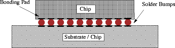
Figure: The figure shows the flip-chip method of interconnection where solder bumps are used to interconnect a chip to a substrate or sometimes to another chip.