Semiconductors were originally packaged in cans, called the `TO Can' or `TO Package,' which is a generic term for a transistor outline package established by an organisation called JEDEC as an industry standard. As the required number of I/O pins began to rise, it became difficult to work with `TO Cans.' As a result, new forms of packages for semiconductor integrated circuits were developed. The following paragraphs provide a brief overview of the commonly used `Level - 1'packaging technologies [1, 5]. These packages are classified according to their mounting method as follows (see Figure ![]() ):
):
One of the earliest packaging standards was the rectangular DIP. It has been the main stream of the microelectronics industry since 1968 and still accounts for some 80% of all integrated circuit packaging [5, 1]. The DIP has I/O leads which extend from two opposite sides of the package and are bent downward as shown in Figure ![]() .
.
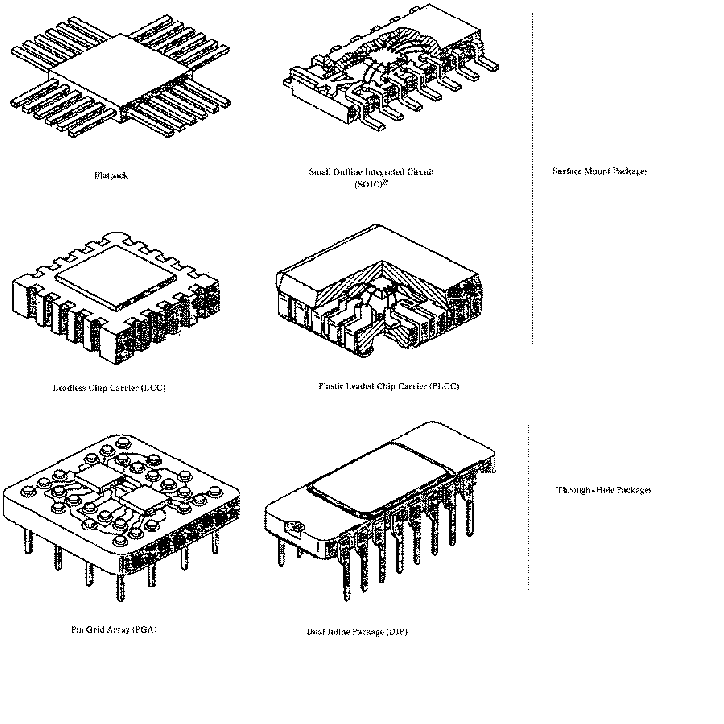
Figure: Common package outlines. In all of these packages there is a microelectronic circuit with on-chip pads. These pads are connected to package leads or terminals through one of the interconnection technologies described before. `Leadless' pertains to electronic devices that do not have electrical leads extending from their enclosures but rather to solder `lands' or `bumps' located on the top, bottom, or sides of the package.
With the advances in VLSI technology, the lower available pin counts of the rectangular DIP have become a limiting factor. With pins spaced 2.4 mm apart on only two sides of the package, the physical size of the DIP has become too great. On the other hand, the physical size of an unpackaged microelectronic circuit (bare die) has been reduced to a few millimetres, which in turn has led to reduced power consumption and chip delay time due to greater circuit integration -thus reducing the cost per circuit function. As a result the DIP package has become up to 50 times larger than the bare die itself, thus defeating the objective of shrinking the size of the integrated circuits.
Another type of packaging which requires through hole mounting is the pin grid array (PGA), which is typically used with VLSI chips that require pin counts greater than 100. The PGA is often composed of a square, multilayer, ceramic chip carrier with a matrix of butt-brazed through hole pins under its surface. The cost of pin grid array packages is much higher than that of DIPs, because PGAs are made of ceramic and are generally multilayer. However, the PGA provides up to a four fold improvement in pin density over the DIP, when tight array spacing is employed. A typical pitch spacing in this technology is in the order of 0.4 to 0.5 mm.
A new family of packaging, which requires a different mounting method, has appeared due to the increase in the IC pin count and the requirement for smaller weight and size of the packaged circuits. This packaging family, called surface-mounted technology (SMT), consists of soldering the leads on the surface of the PCB instead of utilising through hole-mounting as shown in Figure ![]() . This family of packaging has overcome some of the space problems associated with through hole mounting and the low pin count in DIPs.
. This family of packaging has overcome some of the space problems associated with through hole mounting and the low pin count in DIPs.
One of the earliest members of the surface-mounted family is the flatpack package. It is similar to the DIP with the exception that the leads protrude outward to form a flat surface and are mounted on pads, in order to obviate through hole-mounting. Flatpacks are found in (i) a dual in-line pin configurations called small outline integrated circuits (SOIC) and (ii) a configuration with leads which protrude on all four sides of the component package. SOICs typically have gull wing-type leads and are preferred for lead counts of up to 20 pins. The pitch spacing in the SMT is in the order of 1 mm as opposed to 2.4 mm for DIPs.
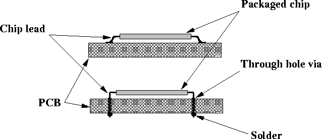
Figure: A generic schematic diagram showing the difference between the surface mount technology (upper) and through hole mounting (lower).
Another type of package is called the chip carrier. It has a square structure with I/O connections on all four sides of the package. There are three main types of chip carriers: ceramic, plastic leaded and leadless ceramic chip carriers (LCCCs, usually called LCCs - for brevity), as shown in Figure ![]() . Chip carriers offer higher packaging densities compared to the DIPs and more I/O terminals of up to 300 pins. In addition, LCCs require a typical pitch size of 0.6 to 0.8 mm, which is 70% less compared to the DIP.
. Chip carriers offer higher packaging densities compared to the DIPs and more I/O terminals of up to 300 pins. In addition, LCCs require a typical pitch size of 0.6 to 0.8 mm, which is 70% less compared to the DIP.