The basic idea behind developing MCM technology is to decrease the average spacing between ICs in an electronic system. Therefore, the fundamental aspect of MCM technology is chip interconnection, which includes connecting I/O conductors on a chip to an MCM substrate. The goals are higher performance resulting from reduced signal delays between chips, improved signal quality between chips, reduced overall size and reduced number of external components [7, 8].
An MCM substrate can be composed of different layers and their number depends on the MCM technology used. These layers provide all the interconnections between the different mounted ICs in addition to the interconnections needed to interface for ``Level - 2'' packaging using any of the interconnection technologies discussed in section ![]() .
.
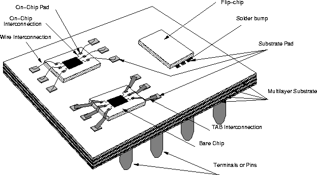
Figure: A generic schematic diagram of an MCM which shows how bare dice are interconnected to an MCM substrate using different interconnection technologies.
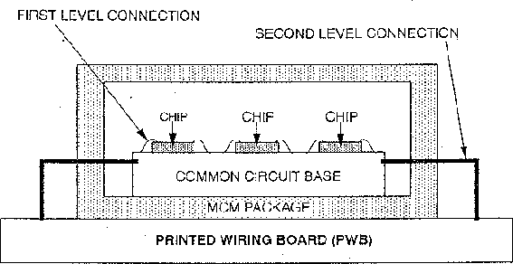
Figure: The basic architecture of MCMs.
The basic architecture of an MCM is composed of:
A schematic diagram which illustrates the above described MCM basic architecture is shown in Figure ![]() . Moreover, Table
. Moreover, Table ![]() shows the relationships between architectural components and the corresponding technologies.
shows the relationships between architectural components and the corresponding technologies.
| LEVEL | FUNCTIONS | TECHNOLOGIES |
| Chips | Digital | Si: CMOS, bipolar |
| Analog | GaAs, CGaAs | |
| Mixed Analog-Digital | ||
| 1st level interconnections | Conductor connection | Peripheral: Wire bond, |
| from chips to common | TAB, flip TAB | |
| circuit base | Area: flip chip, | |
| solder bump, area TAB | ||
| Common circuit base | Signal interconnection | Hybrid circuits |
| Power and Ground | MCM-L, MCM-C, MCM-D | |
| conductors | MCM-D/C | |
| MCM Seal | Hermeticity | Peripheral Conductors: |
| Heat removal | DIP, QFP | |
| Physical protection | Area array conductors: | |
| conductors | PGA | |
| 2nd level connection | Conductor connection | Plated through-hole vias |
| to PWB | surface mount | |
There is a long list of specifications that are used to describe an MCM technology. Some of the main specifications are (see also Figure ![]() ) line pitch; which is defined as the nominal distance from centre to centre of adjacent wires, via pitch; which is the nominal distance from centre to centre of adjacent vias, and the number of layers used in the implementation of an MCM. These parameters will be used in the next section to compare between the different MCM technologies.
) line pitch; which is defined as the nominal distance from centre to centre of adjacent wires, via pitch; which is the nominal distance from centre to centre of adjacent vias, and the number of layers used in the implementation of an MCM. These parameters will be used in the next section to compare between the different MCM technologies.
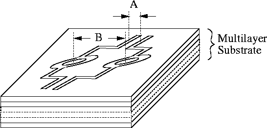
Figure: A schematic diagram illustrating some of the MCM basic parameters.