An interconnection is the conductive path required to achieve connection from one circuit element to another or to the rest of the circuit system. Such interconnections may be pins, terminals, formed conductors, or any other mating system [3, 4].
At the chip level, interconnects are needed to connect the different electronic circuit elements implemented on or in the chip such as transistors, capacitors, etc. For example, a diagram which illustrates the implementation of an `inverter' in a CMOS technology is shown in Figure ![]() . This diagram illustrates the implementation of two electronic elements, an n-MOS and a p-MOS transistor, and how they are interconnected, starting from a schematic diagram and ending with physical implementation.
. This diagram illustrates the implementation of two electronic elements, an n-MOS and a p-MOS transistor, and how they are interconnected, starting from a schematic diagram and ending with physical implementation.
An electronic chip can contain hundreds or thousands of electronic components to perform a certain function as part of an electronic system. As technology progresses, and devices become smaller, the interconnection density (ie. the number of wires per unit area) increases. Therefore, in order to minimise the length of these wires, both inside an IC and in between ICs on a PCB, several layers of interconnections are used. For instance, current IC fabrication technologies commonly allow signals to travel between circuits inside the chip on two or more metal layers, which can be connected to the active layers (eg. polysilicon and diffusion to form transistors) through so-called `contact cuts' (see Figure ![]() ).
).
Printed circuit boards may also comprise several routing layers, sometimes more than 10, in order to allow ICs to be placed close to one another. As illustrated in Figure ![]() , a signal may be re-routed onto another layer through a so-called `via' which is a metal-coated hole in the PCB.
, a signal may be re-routed onto another layer through a so-called `via' which is a metal-coated hole in the PCB.
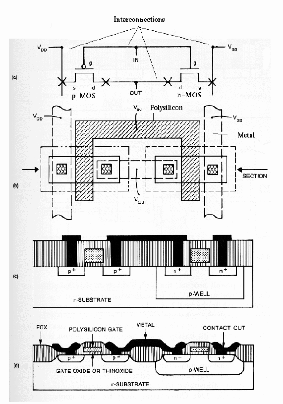
Figure: (a). A schematic circuit diagram of a CMOS inverter which shows the use of either metal or polysilicon as a material to interconnect transistors terminals (d, g and s represent the drain, gate, and source of the transistor, respectively) to the corresponding terminals or to power supply terminals labelled V ![]() and V
and V ![]() . (b) A circuit layout that corresponds to the inverter shown in (a). A cross section of the finished p-well process is shown in (c), while (d) shows a more realistic representative cross-section of the cross section shown in (c).
. (b) A circuit layout that corresponds to the inverter shown in (a). A cross section of the finished p-well process is shown in (c), while (d) shows a more realistic representative cross-section of the cross section shown in (c).
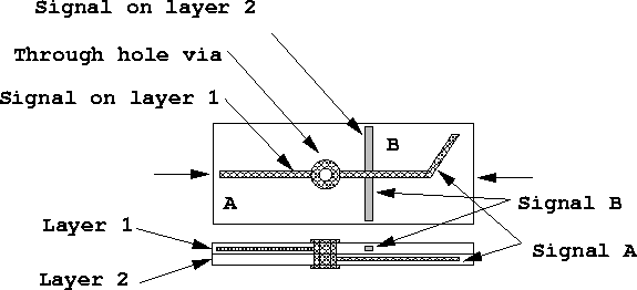
Figure: (upper) A top view of a printed circuit board with two layers showing two signals A and B in two separate layers. (lower) A cross section of the upper schematic showing the two signals in addition to a schematic for a via, which is similar to the through holes used by some types of packages.
The interface between a chip terminal and an interconnect is done through what is called a `pad,' which is an enlarged conducting area on the chip surface created for the purpose of bonding an external interconnect to a chip terminal.
A bare die can be packaged using a number of packaging types depending on the required number of I/O terminals, thermal properties, size, etc. Moreover, a number of interconnection technologies such as wire bonding, tape-automated bonding (or TAB, see section ![]() ), and flip-chip bonding (see section
), and flip-chip bonding (see section ![]() ) technologies can also be used, depending on the requirements. The interconnection between the chip and the package, when wire bonding technology is used, is performed by connecting the pads on the chip surface to the so called `leadframe,' which is simply a rectangular metal frame with leads. After encapsulation or lidding of the package, the frame is cut off, leaving the leads extended from the package, as shown in Figure
) technologies can also be used, depending on the requirements. The interconnection between the chip and the package, when wire bonding technology is used, is performed by connecting the pads on the chip surface to the so called `leadframe,' which is simply a rectangular metal frame with leads. After encapsulation or lidding of the package, the frame is cut off, leaving the leads extended from the package, as shown in Figure ![]() .
.
In a bare chip, the interconnection width (normally accomplished in the polysilicon or metal layers) is in the order of microns, depending on the fabrication technology. Due to manufacturing and mechanical limitations and thermal constraints a typical pad size in a CMOS technology is in the order of 100 ![]() 100
100 ![]() m
m ![]() .
.
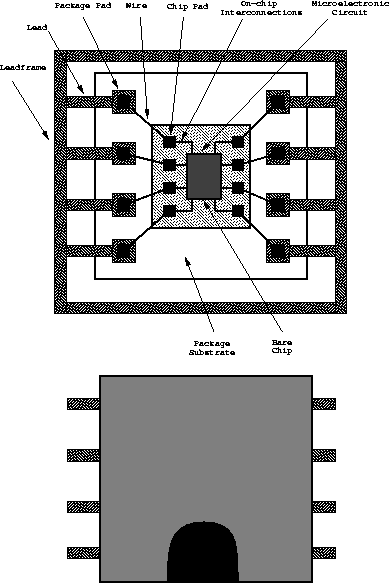
Figure: (upper) A schematic diagram showing how a chip is interconnected to a leadframe using wire bonding technology, the (lower) schematic shows a top view of the packaged chip.