


Next: Interconnect Usability and Accessibility
Up: Advantages of 3D Packaging
Previous: Size and Weight
One of the main issues in packaging technology is the chip footprint, which is the printed circuit board area occupied by the chip (see Figure  ). The term `silicon efficiency' is defined as the ratio of total silicon footprint area to substrate area. Hence, in any 2D technology, the silicon efficiency can never exceed 100% - however, in 3D
technology this barrier is broken due to many overlapping footprints within one stack. In the case of MCMs versus single packages, the footprint is reduced by 20-90% because of the use of bare dice (ie. unpackaged dice). A comparison between 3D technology and other packaging technologies in terms of silicon efficiency is shown in Figure , where 3D technology exceeds 100%.
). The term `silicon efficiency' is defined as the ratio of total silicon footprint area to substrate area. Hence, in any 2D technology, the silicon efficiency can never exceed 100% - however, in 3D
technology this barrier is broken due to many overlapping footprints within one stack. In the case of MCMs versus single packages, the footprint is reduced by 20-90% because of the use of bare dice (ie. unpackaged dice). A comparison between 3D technology and other packaging technologies in terms of silicon efficiency is shown in Figure , where 3D technology exceeds 100%.
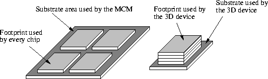
Figure: A graphical illustration of the silicon efficiency between MCMs and 3D technology.
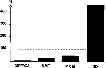
Figure: Silicon efficiency comparison between 3D packaging technology and other conventional packaging technologies (Adapted from [12]).
Next: Interconnect Usability and Accessibility
Up: Advantages of 3D Packaging
Previous: Size and Weight
Said F.
Al-Sarawi,
Centre for High Performance Integrated Technologies and Systems (CHIPTEC),
Adelaide, SA 5005,
March 1997