


Next: Limitations of 3D Packaging
Up: Area Interconnection between Stacked
Previous: Area Interconnection between Stacked
In this method, an array of contacts are used to provide the vertical interconnections between stacked MCMs. There are six variants of this method as follows:
- Fuzz buttons in plastic spacer and filled vias in
substrate: In this method MCMs are stacked with an intermediate layer
called the spacer or fuzz buttons board. This layer has a precision plastic
spacer to provide clearance for chip and bond, and fuzz buttons to provide
interconnection by applying a mating force on the stacked MCMs as shown in
Figure
 .
Fuzz buttons are physically made of fine gold `wire wool' and the integrity
of a contact made by the contact of two of these wool pads is surprisingly
good. This method is developed and used by E-systems for stacking MCMs with
diamond substrates.
.
Fuzz buttons are physically made of fine gold `wire wool' and the integrity
of a contact made by the contact of two of these wool pads is surprisingly
good. This method is developed and used by E-systems for stacking MCMs with
diamond substrates.
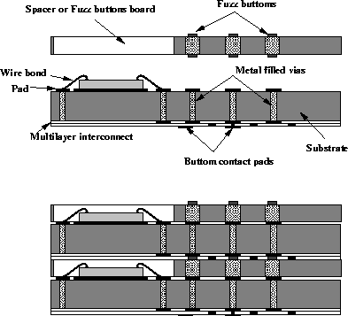
Figure: (upper) A schematic diagram for an array of contacts
between MCMs with through-hole vias. (lower) Two MCMs are stacked by applying
a mating force.
- Elastomericconnectors with electrical feedthroughs:
The vertical interconnections in this method are implemented by a combination
of `electrical feedthroughs' and elastomeric connectors. The `electrical feedthroughs'
are premanufactured elements
 that
are mounted into a laser structured substrate by an embedding technique. A
schematic diagram of this method is shown in Figure .
This method was developed by the Research Center of Microperipheric Technologies
at the Technical University of Berlin. In addition, Texas Instrument has used
a variant of this method in the design of a high performance parallel computer
called `Aladdin Parallel Processor.'
that
are mounted into a laser structured substrate by an embedding technique. A
schematic diagram of this method is shown in Figure .
This method was developed by the Research Center of Microperipheric Technologies
at the Technical University of Berlin. In addition, Texas Instrument has used
a variant of this method in the design of a high performance parallel computer
called `Aladdin Parallel Processor.'
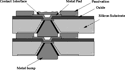
Figure: Two wafers stacked using filled vias method.
Next: Limitations of 3D Packaging
Up: Area Interconnection between Stacked
Previous: Area Interconnection between Stacked
Said F.
Al-Sarawi,
Centre for High Performance Integrated Technologies and Systems (CHIPTEC),
Adelaide, SA 5005,
March 1997