The stacked ICs are flipped and interconnected to either a substrate or another chip using the solder joint technology discussed in section ![]() . This technique was used by Fujitsu [24] for stacking a GaAs chip on a CMOS chip technology as illustrated in Fig.
. This technique was used by Fujitsu [24] for stacking a GaAs chip on a CMOS chip technology as illustrated in Fig. ![]() . (See also section
. (See also section ![]() ).
).
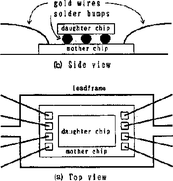
Figure: A schematic diagram of Fujitsu GaAs on Si PLL Frequency Synthesiser IC.