


Next: Thin Film Conductors on
Up: Periphery Interconnection between Stacked
Previous: Periphery Interconnection between Stacked
This is similar to the solder edge conductor for ICs, discussed in section  . However, in this case the vertical interconnections are performed between MCMs rather than ICs. There are two variants of this method:
- Solder dipped stacks to create vertical conductors on edge: This technique is similar to the solder dipped stacks to create vertical conductors on edge technique discussed in section with the exception that MCMs are used to form the stack. This technique was used by Trymer in the development of a guidance system for hypervelocity projectiles.
- Solder leads on stacked MCMs: After each MCM is packaged separately they are stacked with the leads formed to allow stacking as shown in Figure , then soldered for permanent mounting. Matsushita has used this method in the design of high density SRAMs and DRAMs by using 2-8 layer stack. This method is referred to as ``Stacked QFP- format MCMs'' because the leads on the bottom board are formed as a quad-flat pack package (for more information refer to section ).
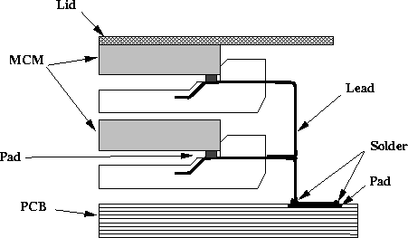
Figure: A soldered leads on stacked MCMs vertical interconnection method, which is a variant of the solder edge conductors method discussed in section .
Next: Thin Film Conductors on
Up: Periphery Interconnection between Stacked
Previous: Periphery Interconnection between Stacked
Said F.
Al-Sarawi,
Centre for High Performance Integrated Technologies and Systems (CHIPTEC),
Adelaide, SA 5005,
March 1997