


Next: Interconnection Topology
Up: Introduction
Previous: Objective
A number of countries have recognised the importance of electronic packaging technologies (such as the United States, Japan and some European countries). However, the level of advancement and development in electronic packaging is lagging behind the advances in microelectronics. This is due to the inherently multi-disciplinary field of electronic packaging, which incorporates several of the traditional sub-areas of mechanics, electronics, physics and chemistry. The most prominent of these areas are heat transfer, materials, signal transmission, mechanical analysis and manufacturing.
Most electronic applications require increased reliability and performance as well as lower cost, weight and size. All of these factors depend on the capabilities related to making more integrated components, which in turn depend on advanced assembly equipment that can put a large number of small components into smaller and smaller areas.
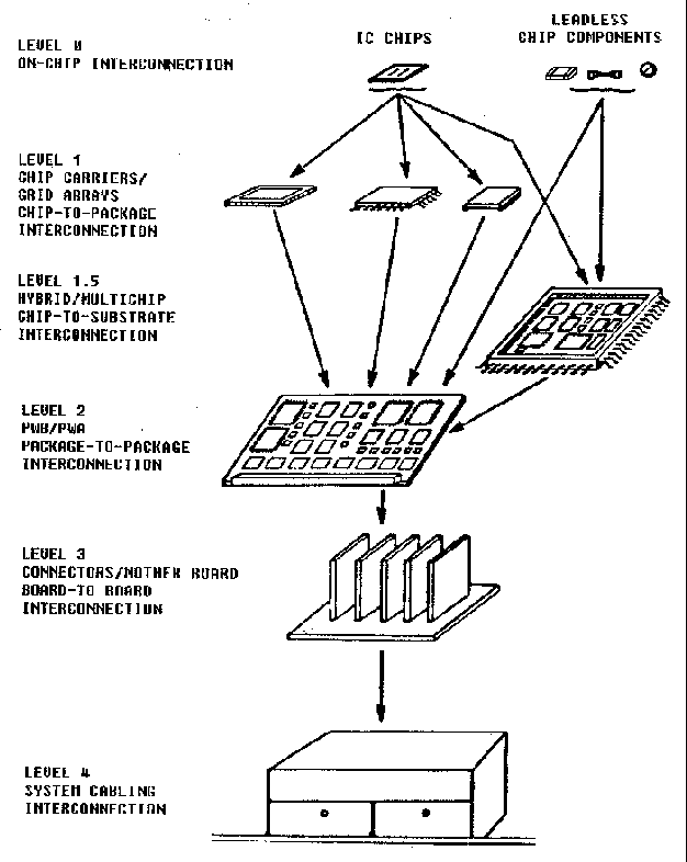
Figure: Bottom-up packaging and interconnection levels of a generic electronic system.
A general electronic system could be classified into four packaging or interconnect levels, as shown in Figure  [1, 2]. These packaging and interconnection levels are:
- Level - 0:
- This level involves interconnecting different electronic elements such as transistors, resistors, capacitors, etc, on the same chip with no packaging. Physically, this microelectronic circuit is called a `bare die' or `bare chip.'
- Level - 1:
- Pertains to all processes (eg. mounting, bonding and encapsulating) involved in packaging a bare die to produce an integrated circuit (IC).Wiring the die to a package usually involves one of the interconnection methods discussed in section .
- Level - 2:
- Pertains to all the technologies employed in interconnecting a number of such `integrated circuits' on a printed circuit board
 (PCB).
- Level - 3:
- Pertains to the interconnection of the boards into a cabinet system.
- Level - 4:
- Pertains to the cabling interconnections and housing of the final system.
The discussion throughout this report will concentrate on `Level - 1' and `Level - 1.5.' `Level - 1.5' is an intermediate level between `Level - 1' and `Level - 2' and is concerned with mounting packaged chips to what is called a `multichip module' (illustrated later in section ). A typical microelectronic package is designed to provide the following functions [1]:
- Connections for signal lines leading onto and off the silicon chip.
- Connections for power lines that powers the circuits on the chip.
- Connections of signal lines between the system components and interconnections for input/output terminals.
- Removal of the heat generated by the circuits.
- Support and protection of the bare chip.
There are a large number of requirements that an electronic package has to fulfill, such as:
- Mechanical requirements: These may involve constraints on the structure and thermal characteristics of the supporting substrate. The substrate is a base material that provides a supporting surface for deposited or etched wiring patterns - for attachment of component parts, or for fabrication of a semiconductor device.
- Input/Output (I/O) requirements: These vary significantly depending on the system of interest. For example, the I/O ports for a hand-held calculator are the keyboard and the display. By contrast, in a large computer system the I/O ports may include tape drives, disk drives, printers, etc.
- Environmental requirements: Tolerance of the packaging to operating conditions such as air humidity and exposure to chemicals.
- Reliability requirements: The system's ability to operate for many years with very few problems.
- Interconnection requirements: The number of I/O ports that are needed to provide inter-chip communication, ie. between chips and the supporting substrate.
Next: Interconnection Topology
Up: Introduction
Previous: Objective
Said F.
Al-Sarawi,
Centre for High Performance Integrated Technologies and Systems (CHIPTEC),
Adelaide, SA 5005,
March 1997